
Top 10 design rules for flex and rigid-flex PCBs
As electronics become smaller, lighter, and more complex, flexible printed circuits (FPCs) and rigid-flexible printed circuit boards (RFPCBs) have become the preferred choice for leading product designers. From aerospace and medical devices to wearables, industrial sensors, and new energy applications, these technologies offer versatility where traditional rigid boards fall short.
However, designing flex and rigid-flex PCBs requires more than just copying rigid board techniques. It demands a deep understanding of mechanical stresses, material properties, and manufacturability. To help you succeed, here are CEE PCB’s Top 10 design rules for flex and rigid-flex PCB success.
1. Define flex and rigid areas
Start by clearly distinguishing which areas of the board will be flexible and which will be rigid. This will affect material selection, stack-up design, bend reliability, and component placement. Early planning reduces the need for costly redesigns later. Rigid areas can be just mechanical stiffeners or traditional FR4 material that include areas with standard PTHs (Plated Thru Holes).
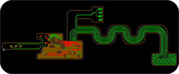
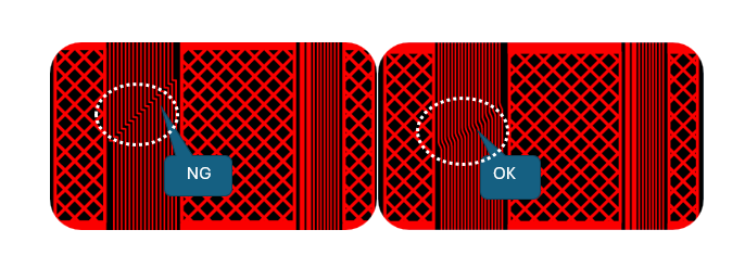
2. Avoid right angles in bend areas
Acute angles create stress concentration points. In flex zones, use curved traces or bends at obtuse angles to prevent cracking or delamination. Smooth routing ensures better mechanical durability, especially over repeated bends.
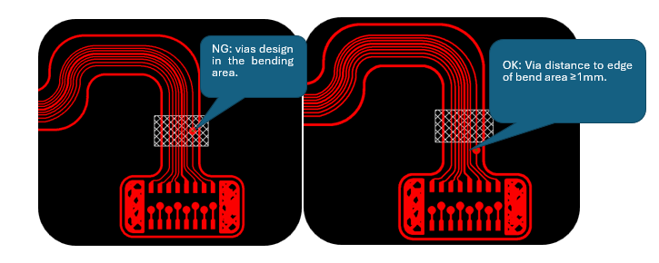
3. Keep vias out of flex zones
Placing vias in bend regions weakens the structure and increases failure risk. Vias should only be used in rigid areas or stiffened zones unless specifically designed for dynamic flexing (which requires advanced materials and testing).
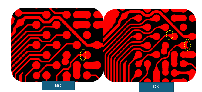
4. Use tear drops and anchor stubs
When transitioning traces to pads that contain plated vias, teardrop shapes help reduce stress and improve mechanical reliability. Anchor stubs on pads in flex regions can prevent pad lifting under flex stress.
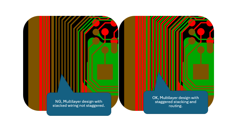
5. Stagger traces across layers
In multilayer designs, don’t stack traces vertically in the flex zone. Instead, stagger them between layers to reduce the risk of stress fractures and improve flexibility. This design technique also reduces impedance mismatches in signal lines.
6. Select correct bend radius
Minimum bend radius is critical. As a general rule for single layer with 18µm copper
- For static bends: radius ≥ 6× the flex thickness(B≥6*A)
- For dynamic bends: radius ≥ 10× the flex thickness(B≥10*A)
Tighter bends increase the risk of cracking, especially with copper conductors.
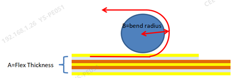
All values are valid for 18µm copper material.
7. Avoid placing components in flex areas
Unless absolutely necessary, keep components out of the flexible regions. Place components on rigid sections to prevent solder joint fatigue and mechanical failures. If components must be on flex areas, then use stiffeners to support the components.
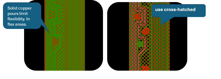
8. Use hatched ground planes in flex zones
Solid copper pours limit flexibility. In flex areas, use cross-hatched ground planes to maintain EMI shielding while preserving bendability. Just ensure continuity and signal return paths are not compromised.
9. Optimise stack-up for balanced flex
Use symmetrical stack-ups with adhesiveless base materials whenever possible. This will improve flex life and reduce unwanted curls. Ensure copper weights and coverlay materials are properly selected to match your bend performance requirements.
10. Collaborate with your manufacturer in an early design stage
Flex and rigid-flex PCBs typically have tighter manufacturing tolerances than traditional rigid PCBs. Early Design for Manufacturability (DFM) reviews with CEE PCB will prevent common design issues and speed up prototyping stages. We will help to optimise yield, cost, and performance.
Final thoughts
Flex and rigid-flex PCBs open new possibilities – but only when designed with care. Following these rules helps ensure your design works not just electrically, but also mechanically.
Product Spotlight
R30-3002002
Harwin

| SKU: | 952-1510-ND |
|---|---|
| Stock: | 5925 |
| Cost: | $0.72 |
NRF54L15-QFAA-R
Nordic Semiconductor
| SKU: | |
|---|---|
| Stock: | 0 |
| Cost: | $2.39 |
STDRIVEG611Q
STMicroelectronics
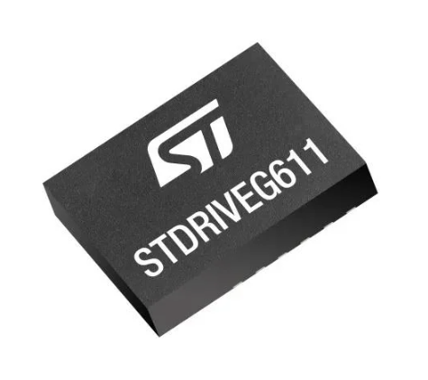
| SKU: | 497-STDRIVEG611QTR-ND |
|---|---|
| Stock: | 0 |
| Cost: | $2.63 |
TBF10SL-4PS-B
ITT Interconnect Solutions
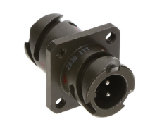
| SKU: | |
|---|---|
| Stock: | 50 |
| Cost: | $44.62 |
CAA572C0G3A663J640LJ
TDK Corporation
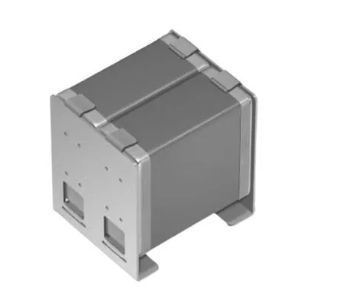
| SKU: | |
|---|---|
| Stock: | 1037 |
| Cost: | $9.16 |
RA1113112R
E-Switch, Inc.
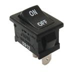
| SKU: | |
|---|---|
| Stock: | 4290 |
| Cost: | $0.00 |


